Select Language:
Scientists have identified a simpler method to produce a rare form of silicon that could enhance batteries and electronic devices while cutting manufacturing expenses. This breakthrough has the potential to save significant amounts of energy during production, making it appealing for future industrial applications. The research was conducted by an international team, including scientists from the U.S. Department of Energy’s Oak Ridge National Laboratory (ORNL), and their findings appeared in the journal Materials Today.
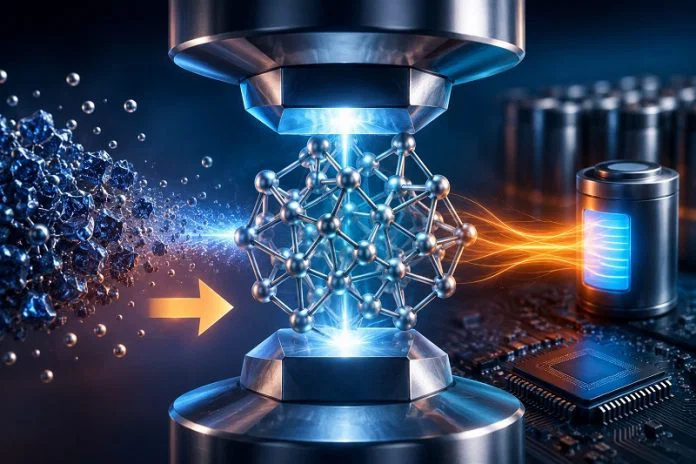
Silicon, second only to oxygen in abundance on Earth, is already widely used in electronics and batteries due to its low cost and excellent electrical conductivity. However, researchers have been particularly interested in a rare silicon allotrope called R8, which could further increase the efficiency of batteries and electronic components. The challenge has been that R8 silicon does not naturally occur. Previously, producing it involved crushing regular crystalline silicon under extremely high pressure—an expensive, complex, and energy-intensive process unsuitable for large-scale manufacturing.
To address this, the team explored an alternative approach. Instead of starting with crystalline silicon, they used amorphous silicon, a more disorganized form with a glass-like structure. Because its atoms are arranged randomly rather than in a regular pattern, amorphous silicon is much more adaptable when pressure is applied. The researchers discovered that compressing amorphous silicon at room temperature, using about 25% less pressure than traditional methods, naturally caused it to transform into the R8 crystal structure.
This process, described as “density matching,” involves increasing the material’s density until its atoms spontaneously align into the R8 structure—similar to pieces of a puzzle fitting perfectly without forcing. To observe this transformation, the team used advanced instruments that direct neutrons and X-rays at the material, enabling them to monitor atomic changes in real time during compression. Complementary computer simulations confirmed their experimental results, modeling atomic behavior under different pressures and showing consistency with observed transformations.
The simulations explained why this method is so effective. The flexible, amorphous structure of silicon allows its atoms to directly rearrange into the R8 form, bypassing multiple complicated intermediate steps that crystalline silicon must go through. The researchers also applied this technique to germanium, another semiconductor used in fiber-optic systems and electronics, and found that the density-matching approach worked there too. This indicates the method might extend beyond silicon, potentially enabling more efficient production of various advanced materials.
If scalable, this process could lower manufacturing costs, reduce energy consumption, and enable wider access to high-performance materials for next-generation batteries and electronics, paving the way for more sustainable and affordable technological advancements.