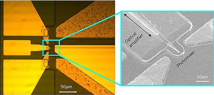
Scientists have made a significant advance in miniaturizing powerful terahertz technology by integrating many of its core functions onto a single semiconductor chip. This milestone, achieved by researchers at UCLA, could pave the way for faster wireless networks, enhanced medical imaging, improved security scanners, and more sophisticated remote sensing tools.
Published in Nature Communications, the research highlights how terahertz waves—the often-overlooked part of the electromagnetic spectrum between microwaves and infrared light—hold immense potential. These high-frequency waves can transmit vast amounts of data and generate detailed images. They are envisioned to enable future ultra-fast wireless communication, detect concealed objects in security screenings, advance environmental monitoring efforts, and even facilitate non-invasive medical diagnostics without harmful radiation.
Despite their promise, terahertz systems have remained largely confined to research settings due to their complexity. Current setups rely on numerous individual components—lasers, amplifiers, signal generators, detectors, and modulators—that must be precisely assembled and synchronized. This intricate assembly makes mass production challenging and limits practical use in everyday devices.
The UCLA team demonstrated that many of these discrete components could be integrated into a single chip using techniques already common in the photonics industry. Photonics, which employs light rather than electricity for information processing and transmission, offers higher speeds and lower energy consumption compared to traditional electronic systems. This development could have a similar impact on terahertz technology as integrated circuits did for computers. Early computers used sprawling rooms full of components, but combining those components onto compact chips revolutionized computing, leading to modern smartphones, laptops, and countless consumer electronics.
A central feature of this new chip design is the use of quantum wells—ultra-thin layers of semiconductor material precisely engineered to manipulate light behavior. These quantum wells are already standard in many modern photonic devices, making them a practical choice for scalable manufacturing. The researchers found that these structures could perform multiple functions simultaneously: generating, detecting, amplifying, and controlling terahertz signals within the same chip. They utilized a technique known as gain-enhanced interband photomixing, where interactions between two laser beams produce terahertz waves at specific frequencies.
In tests, the chip efficiently generated terahertz signals while also detecting them with high sensitivity, outperforming many existing terahertz systems based on photonics. While further development is necessary before commercialization, this research demonstrates a promising pathway toward miniaturized, scalable terahertz devices.
By consolidating complex laboratory equipment onto a single chip manufactured with established techniques, this breakthrough could accelerate the integration of terahertz technology into real-world applications, revolutionizing communications, imaging, and sensing systems in the near future.